Файл:Ebers-Moll model schematic (NPN).svg
Перейти до навігації
Перейти до пошуку

Розмір цього попереднього перегляду PNG для вихідного SVG-файлу: 250 × 175 пікселів. Інші роздільності: 320 × 224 пікселів | 640 × 448 пікселів | 1024 × 717 пікселів | 1280 × 896 пікселів | 2560 × 1792 пікселів.
Повна роздільність (SVG-файл, номінально 250 × 175 пікселів, розмір файлу: 65 КБ)
| Відомості про цей файл містяться на Вікісховищі — централізованому сховищі вільних файлів мультимедіа для використання у проектах Фонду Вікімедіа. |
.svg)
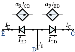
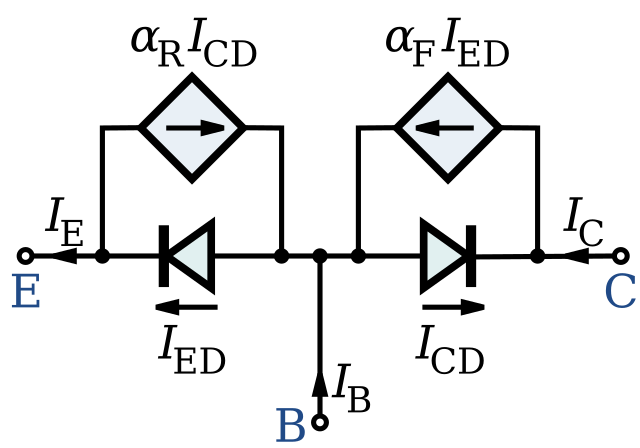
| Опис | A schematic diagram of the Ebers-Moll models of an NPN BJT. The base, collector and emitter currents are IB, IC and IE, the common-base forward and reverse current gains are αF and αR, and the collector and emitter diode currents are ICD and IED. |
| Час створення | (UTC) |
| Джерело | |
| Автор |
|
Цей файл ліцензований на умовах ліцензії Creative Commons Attribution-Share Alike 3.0 Unported
- Ви можете вільно:
- ділитися – копіювати, поширювати і передавати твір
- модифікувати – переробляти твір
- При дотриманні таких умов:
- зазначення авторства – Ви повинні вказати авторство, надати посилання на ліцензію і вказати, чи якісь зміни було внесено до оригінального твору. Ви можете зробити це в будь-який розсудливий спосіб, але так, щоб він жодним чином не натякав на те, наче ліцензіар підтримує Вас чи Ваш спосіб використання твору.
- поширення на тих же умовах – Якщо ви змінюєте, перетворюєте або створюєте іншу похідну роботу на основі цього твору, ви можете поширювати отриманий у результаті твір тільки на умовах такої ж або сумісної ліцензії.
Журнал завантажень локального файлу
This image is a derivative work of the following images:
- File:Ebers-Moll_Model_NPN.PNG licensed with Cc-by-sa-3.0-migrated-with-disclaimers, GFDL-en
- 2010-03-28T19:03:03Z CosineKitty 527x254 (13194 Bytes) Removed incorrect "+" and "-" symbols: charge carriers were backwards for NPN.
- 2010-03-28T18:44:20Z CosineKitty 527x254 (14276 Bytes) Made the following changes to fix errors in the diagram. These changes are based on the diagram on page 903 in ''Microelectronic Circuits, second edition'' by Adel S. Sedra and Kenneth C. Smith, ISBN 0-03-007328-6. 1. Revers
- 2007-09-16T00:43:26Z Kved 527x254 (10811 Bytes) {{Information |Description=NOTE: The diagram has an error. The current through the Base-to-Collector diode should be ICD, not IED. == Summary == Drawn using "Klunky" and added the minor details using MS-WORD |Source=Originall
Uploaded with derivativeFX
Історія файлу
Клацніть на дату/час, щоб переглянути, як тоді виглядав файл.
| Дата/час | Мініатюра | Розмір об'єкта | Користувач | Коментар | |
|---|---|---|---|---|---|
| поточний | 04:24, 28 жовтня 2011 | | 250 × 175 (65 КБ) | Ea91b3dd | Corrected the labels on the dependent current sources. They current I subscripts were swapped. |
| 04:48, 4 серпня 2010 |  | 250 × 175 (31 КБ) | Inductiveload | {{Information |Description=A schematic diagram of the Ebers-Moll models of an NPN BJT. The base, collector and emitter currents are ''I''<sub>B</sub>, ''I''<sub>C</sub> and ''I''<sub>E</sub>, the common-base forward and reverse current gains are ''α''<su |
Використання файлу
Така сторінка використовує цей файл:
Глобальне використання файлу
Цей файл використовують такі інші вікі:
- Використання в ar.wikipedia.org
- Використання в en.wikipedia.org
- Використання в fr.wikibooks.org
- Використання в he.wikipedia.org
- Використання в zh.wikipedia.org
.svg)